


How I Found Nanoscience
As told by Mildred S. Dresselhaus
My early years were spent in a dangerous, multiracial, low-income neighborhood in New York City, the daughter of recently arrived immigrant parents, originally from Eastern Europe. My early elementary school memories up through ninth grade are of teachers struggling to maintain class discipline with occasional coverage of academics, but the students did learn how to survive under difficult circumstances. In my favor was a brother who was a child prodigy in both academics and violin. Being the younger sister, I was also receiving free violin lessons by the time I started elementary school.

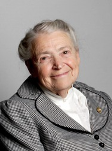
Mildred S. Dresselhaus (Photo: Knut Falch).
Through music school, I met parents with high school and college education, and in this way I learned about the only city-wide public high school of high academic standing available at that time to girls.Entrance to the school was by examination, so I wrote away for old examinations and through self study I was able to pass the examinations, to gain entry to this special high school, and to receive an excellent high school education. In this way I got to Hunter College, with the intention of becoming a school teacher.
Lifelong mentor
In my second year at Hunter College, I had a modern physics course from Rosalyn Yalow, who strongly encouraged me to become a physicist, and she became a lifelong mentor. After her PhD, she taught at Hunter College for one semester before she was able to obtain a research position at the Bronx Veterans Hospital, where she went on to do her 1977 Nobel-Prize-winning work on radio-immuno assays. Rosalyn strongly advised me to study physics at a top graduate school, and she wrote letters of recommendation for my admission to such schools. After one year as a Fulbright fellow at Cambridge University in the UK and a year at Harvard University, I was well prepared for graduate studies in physics at the University of Chicago, where I enrolled at the age of 22.
It was at the University of Chicago that I learned physics in some depth under the Enrico Fermi system. In my first year there I took a course in quantum mechanics from Enrico Fermi, where I learned how to think as a physicist. I got to know Enrico Fermi and his family quite well during that year (1953), which unfortunately turned out to be the last year of his life. He had a great influence on me and on everybody who crossed his path. My PhD thesis was on the microwave properties (measured at a microwave wavelength of 30 cm) of a superconductor in a magnetic field.
At the March 1958 meeting of the American Physical Society I reported some anomalous behavior that could not be explained by the Bardeen-Cooper-Schrieffer theory of superconductivity published in 1957, and this work attracted the attention of Bardeen, Schrieffer, and others and helped my early career. In 1958 I both defended my PhD thesis and married Gene Dresselhaus, whom I had met when we were both at the University of Chicago. I spent the next two years as an NSF postdoc at Cornell University because that was where Gene Dresselhaus had moved to be an Assistant Professor, and there I continued to work on the topic of my PhD thesis.

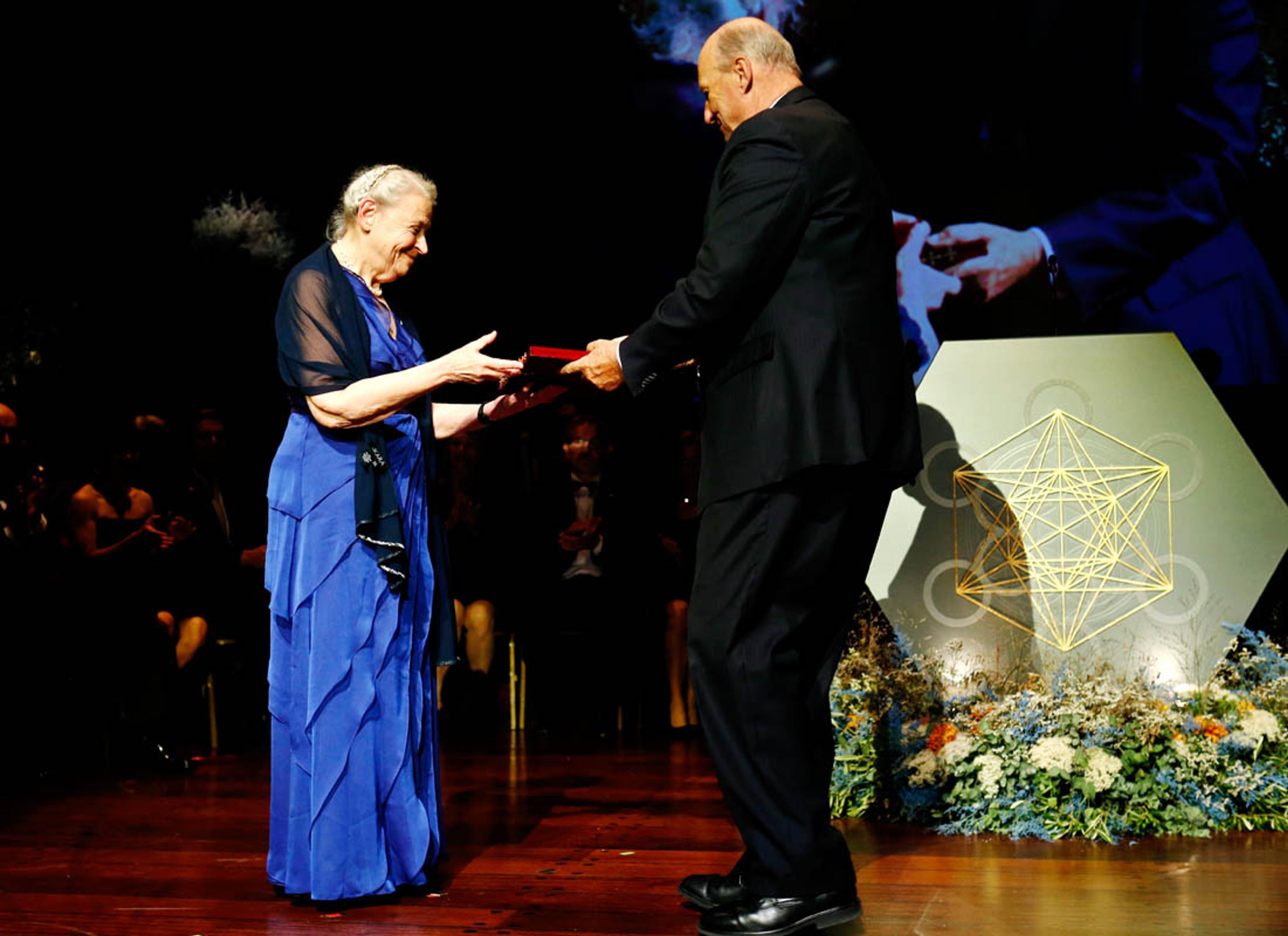
Mildred S. Dresselhaus receives the Kavli Prize from His Royal Highness King Harald at the Oslo Concert Hall (Photo credit: Scanpix).
Combining research and family
My independent career started in June 1960 when Gene Dresselhaus and I both accepted positions at Lincoln Laboratory operated by the Massachusetts Institute of Technology (MIT). Because of the launching of the rocket called Sputnik in 1957, the job market for scientists was good and there were job opportunities for women in physics. Fortunately, Lincoln Laboratory was interested in hiring both of us. There I was asked to change research fields, which in fact turned out to be very rewarding. I was asked to work in the newly emerging field of magneto-optics and chose to do so using semimetals as my materials system, since other workers in the magneto-optics field were strongly focused on studying semiconductors. There were advantages for me to work in a less competitive research area while we had our babies (1959-1964). During my seven years at the MIT Lincoln Laboratory, I studied the electronic structure of the semimetals, graphite, and the group V semimetals. This topic turned out to be very fruitful and interesting and turned out to contribute strongly to the fundamental foundations of condensed matter physics studies on these semimetals. Several physics concepts were investigated in carrying out these studies but my emphasis was on using high magnetic fields and studying electronic structure.
Broader studies became possible when I was invited in 1967 to be on campus at MIT as the Abby Rockefeller Mauzé visiting professor. After a very few months, I was invited to join the permanent MIT faculty as a full professor of Electrical Engineering, to teach classes and to train graduate students for research careers in industry and academia.
Entering the nano world
In 1973 I entered the nano world and started working on intercalation compounds, with the first studies being on the electronic structure, but by 1974 I also got into studies of the vibrational spectra of both donor and acceptor compounds where the graphene layers of the intercalation compound could be doped either p-type or n-type. The staging effect made it possible to synthesize graphene/intercalate superlattices in which the intercalate layer was a single layer of a guest species. However, the carbon layers were either graphene monolayers in the stage 1 compound or graphene bilayers for stage 2 compounds or n graphene layers interlaced with the single intercalate layer in the stage n superlattice. This early work in the 1970s showed that the behavior of monolayer graphene wasdifferent from all the others. Bilayer graphene was also somewhat different, but by the time we reached trilayer graphene the properties of the third-stage compound were almost the same as that of n-layer graphene making an n-stage intercalation compound. However, high-stage intercalation compounds showed some differences in their transport properties relative to pristine graphite because of the significant added charge carrier concentration contributed by the intercalant to the transport properties of the overall intercalation compound. Our research group was heavily involved with preparing and studying all kinds of physical properties associated with the electrons, phonons, and the electron-phonon interaction. This resulted in numerous PhD theses, research papers, and a highly cited review article on graphite intercalation compounds in 1981 that is still actively cited today.
During the second international conference on intercalation compounds in 1980, I met Morinobu Endo, and we started a collaboration that continues until the present, more than 30 years later. He was working on carbon fibers in Japan starting before 1970, and he intercalated these carbon fibers with donor and acceptor species to control their transport properties. Our collaboration allowed his group and my group to do research that would not have been possible without our interaction.

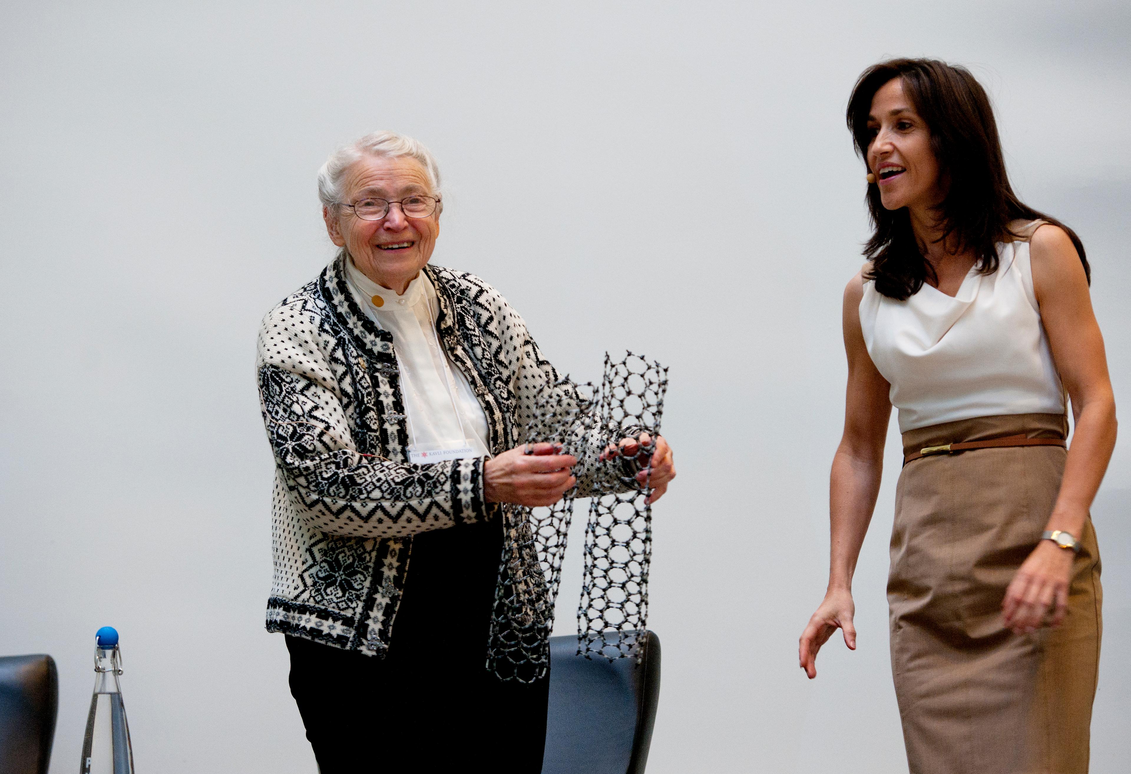
Mildred S. Dresselhaus on stage in Oslo during the Kavli Prize week together with journalist Siri L. Mannes (Photo credit: Scanpix).
Annoyed students
Concurrently my group worked on laser ablation of graphite which produced large carbon clusters. This research eventually was connected to work ongoing at the Exxon research laboratory when I encouraged these researchers to study cluster formation for cluster sizes above 15 carbon atoms. These experiments were also carried out independently in Smalley’s lab at Rice University where Smalley correctly identified the frequently occurring C60 and C70 clusters with fullerenes, which are large molecules made of only carbon atoms. The high symmetry of the C60 molecule was already well known to me from the group theory course I taught at MIT. I still remember assigning a homework problem to my 1984 class asking them to work out the infrared and Raman-active modes of a molecule made of 60 hydrogen atoms located at the 60 vertices of a regular icosahedron. I still remember this assigned problem after almost 30 years, because the students were annoyed with me at that time because I didn’t submit the solution to the problem with the hydrogen atom icosahedron for publication in 1984. After the discovery of C60 in 1985, the next time I taught the course (1986), I had the students calculate the IR active and Raman active modes for C60. This research work got me into a more serious study of the 200 higher-order IR and Raman modes observed in the vibrational mode spectra of C60, and this study was published in a book written with Peter Eklund in the 1990s on fullerenes.
At a Department of Defense–sponsored conference in 1990 in Washington, Smalley was invited to speak on fullerenes and I was invited to speak on carbon fibers. In an ensuing question period we were asked about the connection between a fullerene and a carbon fiber. Since both of us were knowledgeable about each other's work, Smalley suggested that if one elongates C60 along an axis going through a hexagonal face then we get C70, and if we continue this process we would go to C80 and eventually get to what we now call a single wall carbon nanotube.
Controversial result
This idea sounded interesting so I thought about this idea some more. I even talked about the concept at an international conference during the following summer, and found the audience interested in the idea, so much so that when Matsusaka Fujita and Riichiro Saito came to MIT the following year (1991) I suggested that we work out the electronic structure of such single wall carbon tubes to see if such a single wall tube might be interesting. Their calculations showed that such single wall tubes could be either semiconducting or metallic, depending on the orientation of the hexagons relative to the tube axis. This paper was considered to be both interesting and controversial, but I was convinced that the controversial result was correct. Though our paper on this topic was published in 1992, it was not until 1998 when this concept was widely accepted. Of course today, people have forgotten about the years of controversy about this paper.

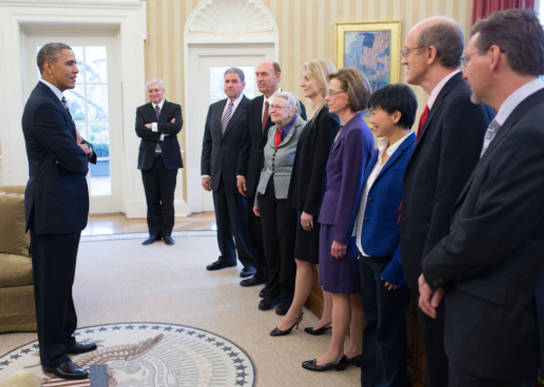
President Barack Obama greets the 2012 U.S. Kavli Prize Laureates in the Oval Office, March 28, 2013. Clockwise from the President: Wegger Chr. Strommen, Norwegian Ambassador to the United States; Rockell N. Hankin, Vice-Chairman of The Kavli Foundation; Robert W. Conn, President of The Kavli Foundation; Kavli Laureates Mildred S. Dresselhaus, Cornelia Isabella Bargmann, Ann M. Graybiel, Jane X. Luu, David C. Jewitt and Michael E. Brown. (Official White House Photo by Pete Souza)
Another turning point
The year 1990 was another turning point in my professional career, when the National Magnet Laboratory moved from the MIT campus to Florida, and I had to abandon high-magnetic-field research. This made me more receptive to trying new research directions. In the area of carbon research, 1990 was the beginning of thinking about single wall carbon nanotubes, and 1991 marks the beginning of our theoretical work on single wall carbon nanotubes as mentioned above. I thus became heavy involved in studying the electrons, phonons, and the electron-phonon interaction in ensembles of nanotubes, and later on moved to doing spectroscopy on individual nanotubes and most recently to doing such spectroscopic studies in graphene.
Also around 1990, the French Navy and the US Navy both became interested in using thermoelectricity for energy harvesting and came to me for input on the possibility of advancing the performance of thermoelectric devices for energy harvesting. In 1992, Lyndon Hicks started his PhD studies at MIT and approached me for a thesis topic, and I suggested that we explore the possibility of using a quantum well, or the quantum confinement concept, to change the fundamental equations governing thermoelectric phenomena. Our simple calculations indicated that this approach was promising. Next we tried the same simple quantum confinement calculation for a quantum wire, and showed that one-dimensional materials would even perform better than two-dimensional materials because of the increase in the boundary scattering of phonons. A third calculation on low-dimensional bismuth showed that semimetallic materials, which had both holes and electrons, also could benefit from the use of low-dimensional samples. For bulk semimetallic materials the negative sign contributions from electrons partly cancel the positive sign contributions from holes. Improved thermoelectric performance was found in quantum-well and quantum-wire materials where sample size could be used to control the thermoelectric properties. All three ideas, in fact, proved to have merit. In 1996, Lyndon Hicks in his PhD thesis also gave experimental proof of the benefit of low-dimensional and nanomaterials for enhancing thermoelectric performance by direct measurements made on two-dimensional thin-film samples. This launched the field of low-dimensional thermoelectricity. In the past 20 years, there has been a rebirth in research and applications of thermoelectric materials for thermal energy management and control. The nanostructured materials have had a significant impact on this technology. Nanostructrual materials now seem likely to become a viable commercial technology in the next decade, judging from the growth of the field in the last five years, both in research and industrial involvement.
New promising ideas
What has been happening in the past two or three years is that new promising ideas have suddenly appeared with several research groups working successfully to enhance thermoelectric performance. Among these new concepts is the introduction of resonant states in the phonon density of states which in turn control the properties of lattice vibrations. These resonant states can be modified by controlling the type of dopant and its concentration through modifying the density of states near the Fermi level in a variety of ways that can be used to increase and better control thermoelectric performance. The introduction of nanometer-size metal particles likewise has been shown to be a promising direction for enhancing thermoelectric performance. A third new idea is modulation doping, whereby grains of two materials are mixed, one material with a high density of dopants and a low carrier mobility and a second material with a low density of dopants and a high carrier mobility. In the resulting two-phase system, the high-dopant-density material releases carriers into the high-mobility material so that phonons can effectively scatter off the increased density of scattering boundaries, while the higher density of electrons can more effectively carry more electrical energy from one contact to the other to produce enhanced thermoelectric performance.
It is thus seen that in both nano-carbons and nano-thermoelectric materials, novel phonon behavior is found. This novel behavior is operative only at the nanoscale. In both nano-carbons and in nano-thermoelectric materials, one with high thermal conductivity (nano-carbons) and the other with low thermal conductivity (nano-thermoelectrics), new and interesting physical phenomena become dominant at the nanoscale. As a result, both areas have become highly active in nanoscience today, both bringing new science concepts along with some promise for eventual practical applications.