


2022 kavli prize in Nanoscience
2022 Kavli
Prize in
Nanoscience
The Norwegian Academy of Science and Letters has decided to award the 2022 Kavli Prize in Nanoscience to Jacob Sagiv, Ralph Nuzzo, David Allara and George Whitesides


"for self-assembled monolayers (SAMs) on solid substrates: molecular coatings to control surface properties"
Committee Members
- Bodil Holst (Chair), University of Bergen, Norway
- Gabriel Aeppli, Paul Scherrer Institut, Switzerland
- Joachim Spatz, Max Planck Institute for Medical Research, Germany
- Naomi Halas, Rice University, USA
- Li-Jun Wan, Chinese Academy of Sciences, China
Citation from the Committee
We interact with materials through their surfaces. The 2022 Kavli Prize in Nanoscience honors four pioneers that created molecular scale coatings for surfaces which enable unprecedented control and engineering of surface properties. Their work transformed surface science and has led to applications shaping our daily lives in areas from medical diagnostics to semiconductor devices.
The concept of organized monolayer films was introduced in the 1930s at liquid-gas interfaces (Langmuir-Blodgett films) [1,2]. In 1946 a process of adsorption of monolayer films on substrates directly from solvents was described [3]. Jacob Sagiv built on these ideas and in 1980 published work which demonstrated unambiguously that molecules with silane termination groups could yield well-defined, covalently bonded monolayer films on surfaces terminated with oxygen [4]. This was a crucial step because most surfaces are coated with a natural oxide layer at ambient conditions. He also showed that different types of molecules could be incorporated within SAMs to modify and/or add functionalities, e.g., fluorescence, and that the physical phenomenon of wetting could be controlled and tailored using SAMs.
In 1983 Ralph Nuzzo and David Allara [5] demonstrated the first SAMs strongly bound to bare metal surfaces. They did this using sulfur-functionalized long carbon chain molecules to create ordered two-dimensional self-assemblies on highly crystalline gold films. They established that SAMs can be characterized by infrared and other optical spectroscopies and deduced the packing and orientation of the SAMs constituent molecules including their functional groups. This generated a deep scientific understanding which enabled the rational design of SAMs with specific functionalities.
George Whitesides and his team were responsible for many innovations which consolidated SAMs as a field of nanoscience and engineering. Of particular significance was the introduction of patterning of, with, and using SAMs [6-8]. With this work they initiated the areas of soft lithography, microcontact printing, and the use of SAMs as resists in lithographic nanofabrication, all crucial enablers of today´s high-tech industries. SAMs are used extensively in medical diagnostics, pharmacology, biosensors, chemical sensors, printers, electronics manufacturing, paints, solar cells, and batteries. There are more than ten thousand SAM-related patents and SAMs have enabled numerous multi-billion-dollar commercial markets.
Jacob Sagiv: For the fabrication of functionalised and mixed monolayer SAMs covalently bonded to oxide surfaces.
Ralph Nuzzo: For the invention of SAMs strongly bound to bare metal surfaces and subsequent experiments exploiting that invention.
David Allara: For determining the molecular structure of SAMs using optical spectroscopies and other characterisation techniques.
George Whitesides: For leading the development of multiple applications and innovations of SAMs, in particular the invention of patterning of, with and using SAMs.
1. Blodgett KB. Films built by depositing successive monomolecular layers on a solid surface. J. Am. Chem. Soc. 1935, 57(1): 1007-1022.
2. Blodgett KB, Langmuir I. Built-up films of barium stearate and their optical properties. Physical Review 1937, 51(11): 0964-0982.
3. W. C. Biglow, D. L. Pickett and W. A. Zisman, Oleophobic Monolayers. I. Films adsorbed from solution in non-polar liquids, Journal of Colloid Science, 1, 513-538, 1946
4. J. Sagiv, Organized Monolayers by Adsorption, 1. Formation and Structure of Oleophobic Mixed Monolayers on Solid Surfaces, J. Am. Chem. Soc., 102, 92-98, 1980
5. R. G. Nuzzo and D. L. Allara, J. Am. Chem. Soc., 105, 4481-4483, 1983
6. Kumar A, Biebuyck HA, Abbott NL, Whitesides GM. THE USE OF SELF-ASSEMBLED MONOLAYERS AND A SELECTIVE ETCH TO GENERATE PATTERNED GOLD FEATURES. Journal of the American Chemical Society 1992, 114(23): 9188-9189.
7. Kumar A, Whitesides GM. FEATURES OF GOLD HAVING MICROMETER TO CENTIMETER DIMENSIONS CAN BE FORMED THROUGH A COMBINATION OF STAMPING WITH AN ELASTOMERIC STAMP AND AN AK.ANETHIOL INK FOLLOWED BY CHEMICAL ETCHING. Applied Physics Letters 1993, 63(14): 2002-2004.
8. Smith RK, Lewis PA, Weiss PS. Patterning self-assembled monolayers. Progress in Surface Science 2004, 75(1-2): 1-68.
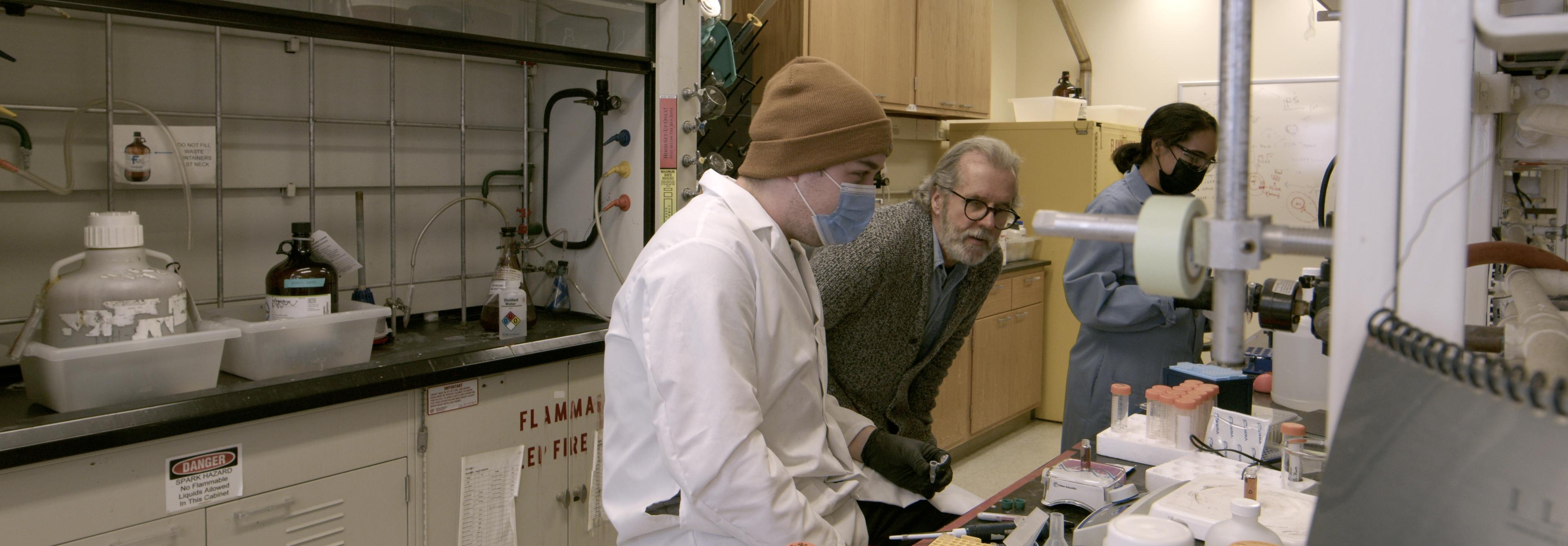
Ralph G. Nuzzo's lab at The University of Illinois at Urbana-Champaign
The power of a molecular monolayer
Imagine the possibility of changing the properties of a material by covering its surface with an extremely thin coating designed to provide a desired functionality. This is precisely the topic of the 2022 Kavli Prize in Nanoscience.
By Fabio Pulizzi, science writer
In making their award, the Kavli Prize in Nanoscience Committee has selected four scientists who contributed to the development of self-assembled monolayers (SAMs): stable and well-organized single layers of molecules that stick to a surface by adsorption and are held together by mutual interaction.
The flexibility of the molecular structures used in SAMs, along with the functionality of their terminal groups, have made SAMs a prolific subject of fundamental research, particularly in the first two decades of the 21st century. As such, SAMs have been translated into applications in a variety of fields, including electronics, photonics, sensing and medicine. The origin of the field is found as far back as the 19th century, however. In 1891, Lord Rayleigh, a well-established chemist who was then interested in the behaviour of oil droplets on water, received a letter from Agnes Pockels, a self-taught German chemist who, fascinated by the behaviour of soap in water, had developed her own tool to study the effect of contaminants on the laminar properties of water. Based on Rayleigh’s recommendation, Pockels’ letter on surface tension was published in the journal Nature [1], and was followed by a number of other contributions by Pockels in the following years.

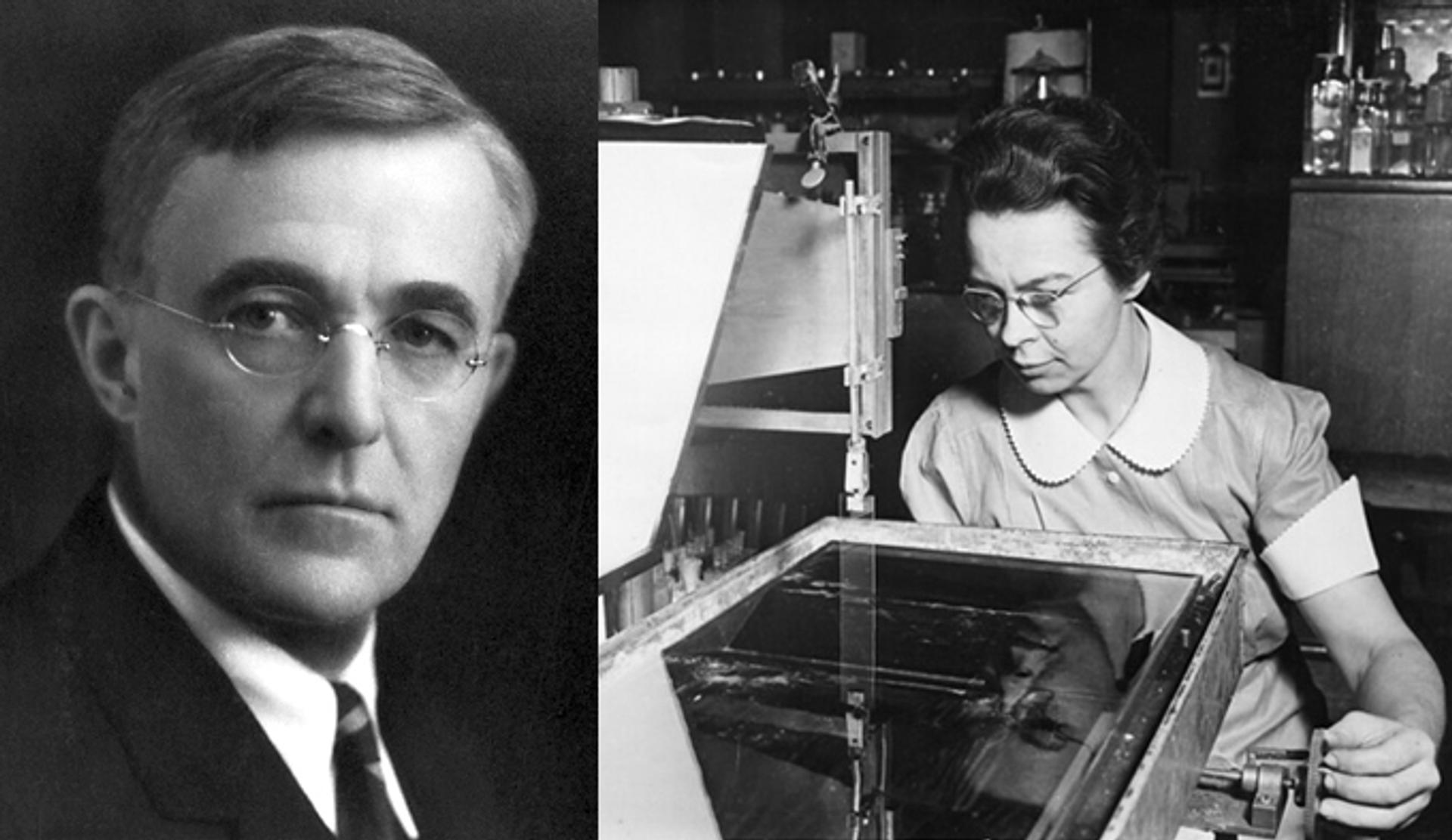
Irving Langmuir and Katharine Burr Blodgett. Credit: Smithsonian Institution
The device conceived and used by Pockels was the precursor of what became the main tool used by Katharine Burr Blodgett: the Langmuir through. Blodgett had worked with her supervisor Irving Langmuir on the deposition of layers of single molecules on a number of surfaces, which became known as Langmuir–Blodgett films. In the early 1930s she developed the instrument that allowed her to deposit very thin molecular layers on metals and glasses, with the first results published in 1935 [2].
Research on Langmuir–Blodgett films continued through the 20th century with the contribution of various scientists, most notably William Zisman and colleagues who, in 1946, demonstrated a process of adsorption of monolayer films on substrates directly from solvents [3], and Hans Kuhn who, towards the end of the 1960s, extended the Langmuir–Blodgett concept to films containing more than one molecular species [4]. The concept of SAMs on solid substrates originated, however, from the work of Jacob Sagiv, who had in fact worked with Kuhn. Towards the end of the 1970s, Sagiv was working at the Max Planck Institut für Biophysikalische Chemie in Göttingen, on leave from the Weizmann Institute in Israel, when he demonstrated that rather than by Langmuir–Blodgett deposition, monolayer films on surfaces could be fabricated by adsorption of molecules on polar surfaces. In his work on “Organized Monolayers by Adsorption” [5], Sagiv showed that molecules including silane groups could covalently bond to surfaces, and proposed that this could be used to create films with controllable molecular organization. This work would in time be adapted for a number of applications, for example in interfacial electron beam lithography (Fig. 1).

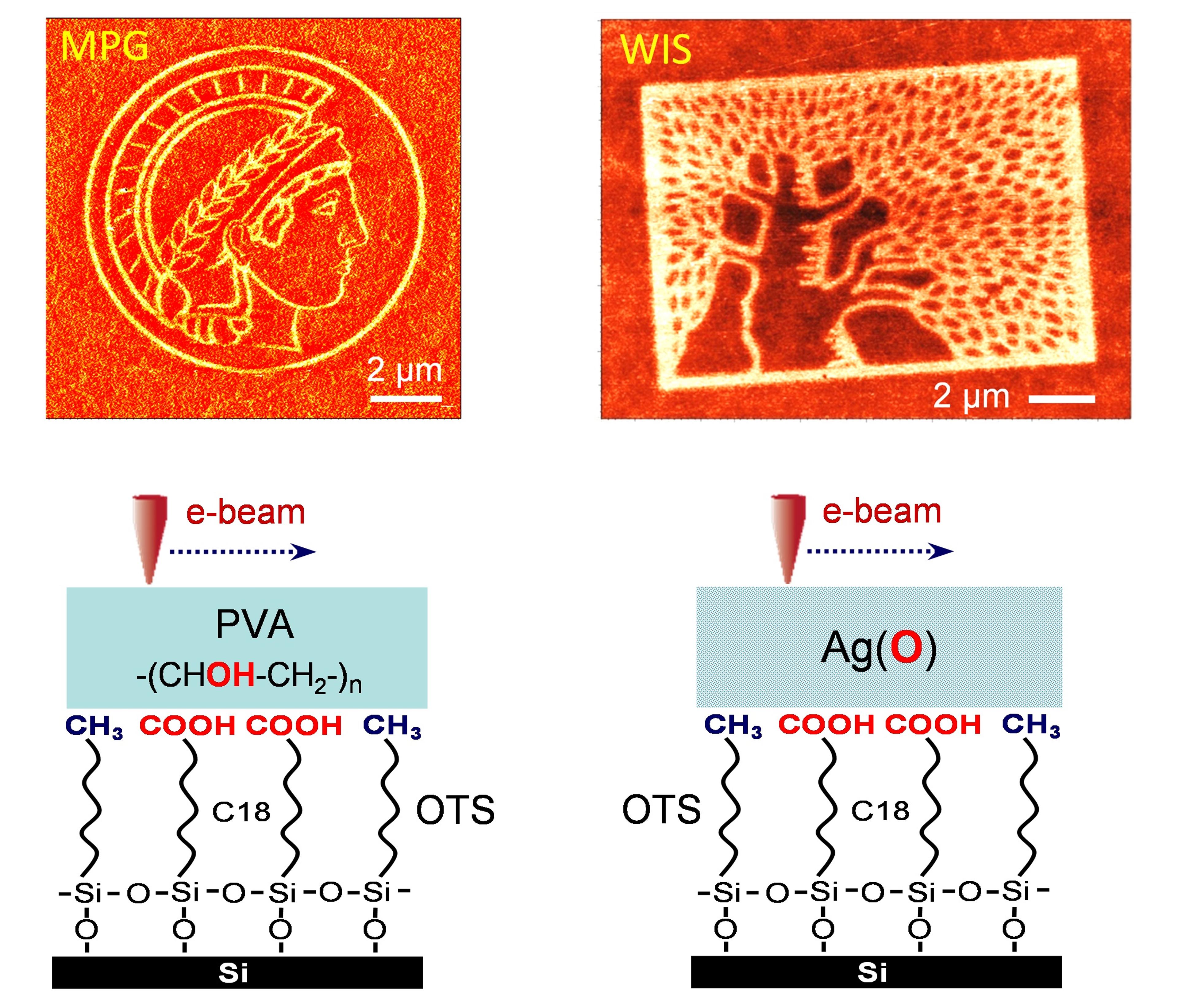
Fig. 1: Examples of nanopatterns fabricated in 2018 by interfacial electron beam lithography applied to organized monolayers by adsorption, first demonstrated by Jacob Sagiv in 1978. The figure shows AFM images of the Max Planck Society logo (left) and Weizmann Institute of Science logo (right) at the nanoscale, and the schematics of the molecular monolayers and the lithographic writing processes used to realize such patterns. Copyright 2022 American Chemical Society - Reprinted (adapted) with permission from Maoz, Berson, Burshtain et al, 2018: Interfacial Electron Beam Lithography: Chemical Monolayer Nanopatterning via Eletron-Beam-Induced Interfacial Solid Phase Oxidation.
In June 1983, Ralph Nuzzo and David Allara, then working at Bell Labs, published another milestone in the field of SAMs [6]: they showed that a large variety of organic molecules would adsorb on a highly crystalline gold substrate, as long as they had a disulphide head group that could bond to gold; the technique was based on the use of molecules having a structure that includes a polar head group and a non-polar tail group. The results were significant for a number of reasons. First of all, the adsorption worked on such a wide range of molecules that one could design a variety of molecular structures with the preferred spatial organization, and, especially, the desired functional group at the tail end of the molecules. Second, Nuzzo and Allara showed that the techniques of ellipsometry and infrared spectroscopy provided an accurate estimate of the thickness and molecular structure of the monolayers, representing a new set of standard characterization tools that would be used in further research and development of SAMs for applications.
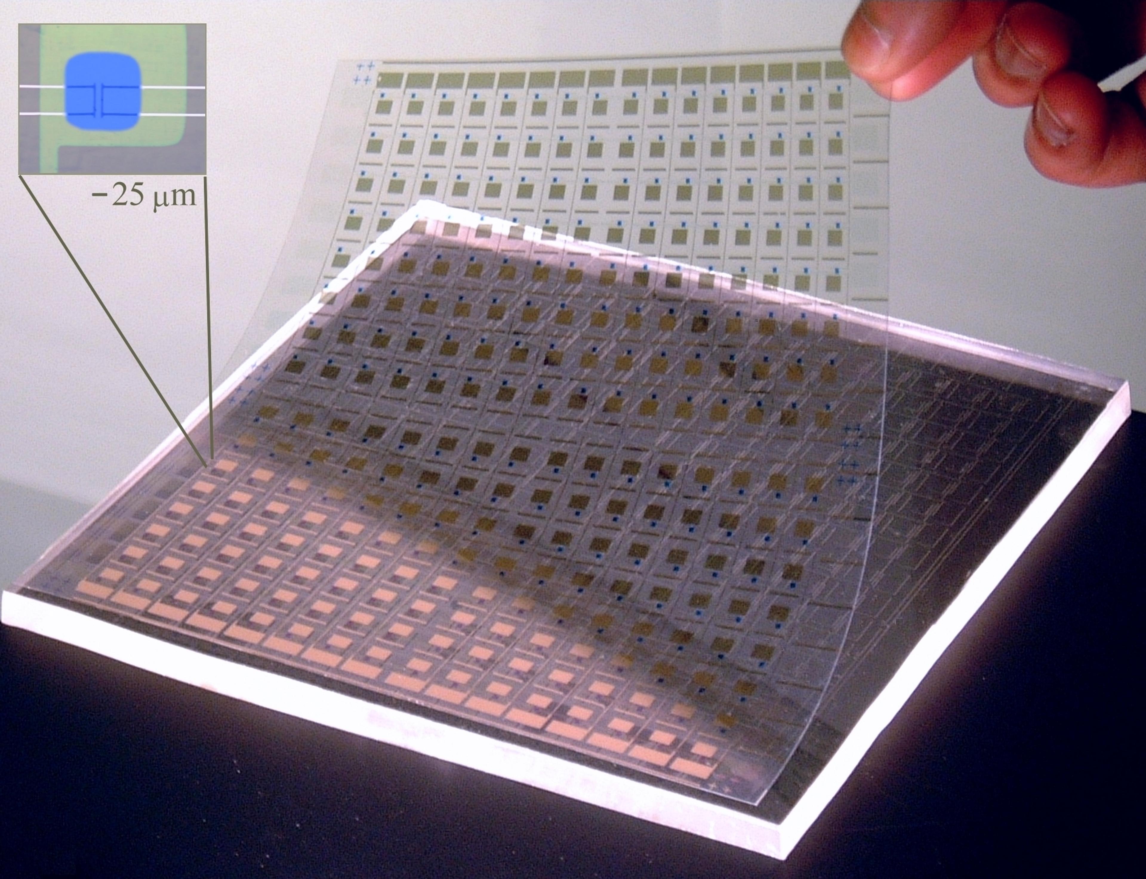
Sagiv, Nuzzo and Allara had laid the foundation to fabricate SAMs films. It was then that George Whitesides, with his group at Harvard, demonstrated that SAMs could have useful applications in the nanometre-scale patterning of surfaces, by creating what became known as soft lithography. The concept of this technique is based on the fact that a metal can be etched away from a substrate if immersed in a suitable reactive agent, but that properly designed SAMs are not affected by that agent. It should then be possible to create a SAM with the required pattern on top of a target metal film, etch away the unprotected metal and finally wash away the SAM to obtain a predesigned metal structure. After the publication in 1992 of the first proof of concept based on a very simple SAM design on a gold film [7], in 1993 Whitesides’ group demonstrated that by using an elastomeric stamp to design the SAM pattern, it was possible to generate gold configurations with different shapes and sizes [8], and to reuse the stamp to produce the same device time after time (Fig. 2).

Figure 2: Image of a flexible plastic active-matrix backplane circuit for an electrophoretic high-contrast display, as fabricated using soft-lithographic patterning methods. The Inset shows an optical micrograph of a typical transistor. The image is courtesy of Professor John A. Rogers, who had worked in George Whitesides’ group, and exemplifies historically important advances in fabrication. These results were reported in PNAS 98, 4835–840 (2001).
The work by Sagiv, Nuzzo, Allara and Whitesides motivated research towards the use of SAMs as films or, alternatively, as templates for patterning films multiple times. The ability to create films of molecules having terminal groups sensitive to other different molecules has motivated the use of SAMs in chemical and biomedical sensors. Furthermore, the precise patterning of SAMs has been used to create electronic and optical devices with very precise patterns.
Beyond fundamental research, SAMs have stimulated a large number of industrial applications. Since 1995 the number of patents related to SAMs has increased steadily, and from 2010 to 2020 between 400 and 500 patents have been filed every year. The simplicity and low cost of SAM-based patterning has especially encouraged patents concerning the fabrication of devices. But perhaps the most impressive fact is the extensive range of fields in which the more than ten thousand patents filed so far are distributed (Fig. 3). The most prolific fields are electronics and biomedical applications, but SAMs are also used in bio- and chemical sensors, energy devices including batteries and solar cells, optics and photonics and even inks and dyes. With a multi-billion-dollar market, it is fair to say that SAMs are one of the outcomes of nanoscience research that have already impacted our lives, and will continue to do so for the foreseeable future.

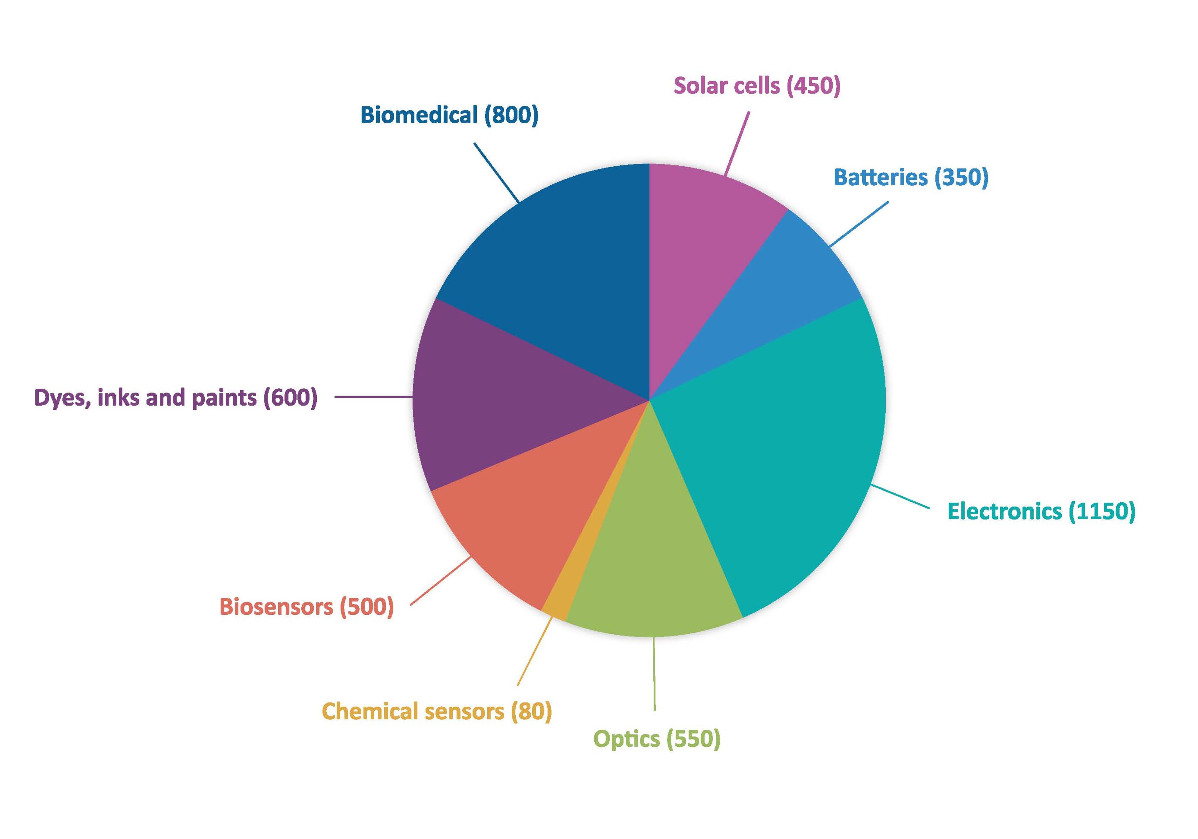
Figure 3: Application sectors of SAMs based on an analysis of patents from worldwide patent offices and with an application date between January 2011 and January 2022. Please note that the same patent can belong to (and thus be counted in) more than one application field reported in the pie chart. Figure by A. Della Pia and D. Magri, Ciaotech/ PNO consultants; analysis based on the Wheesbee platform.
As Professor Bodil Holst of the University of Bergen, and chair of the Kavli Prize in Nanoscience Committee, said “We interact with materials through their surfaces. The 2022 Kavli Prize in Nanoscience honours four pioneers who created molecular-scale coatings. Their work has led to applications shaping our daily lives in areas from medical diagnostics to semiconductor devices.”
References
1. Pockels, A. Nature 46, 437–439 (1891)
2. Blodgett, K. B. J. Am. Chem. Soc. 57, 1007–1022 (1935)
3. Biglow, W. C., Pickett, D. L. & Zisman, W. A. J. Colloid Sci. 1, 513–538 (1946)
4. Kuhn, H. Verhandlungen der Schweizerischen Naturforschenden Gesellschaft 245–266 (1965)
5. Sagiv, J. J. Am. Chem. Soc. 102, 92–98 (1980)
6. Nuzzo, R. G. & Allara, D. L. J. Am. Chem. Soc. 105, 4481–4483 (1983)
7. Kumar, A., Biebuyck, H. A., Abbott, N. L. & Whitesides, G. M. J. Am. Chem. Soc. 114, 9188–9189 (1992)
8. Kumar, A. & Whitesides, G. M. Appl. Phys. Lett. 63, 2002–2004 (1993)